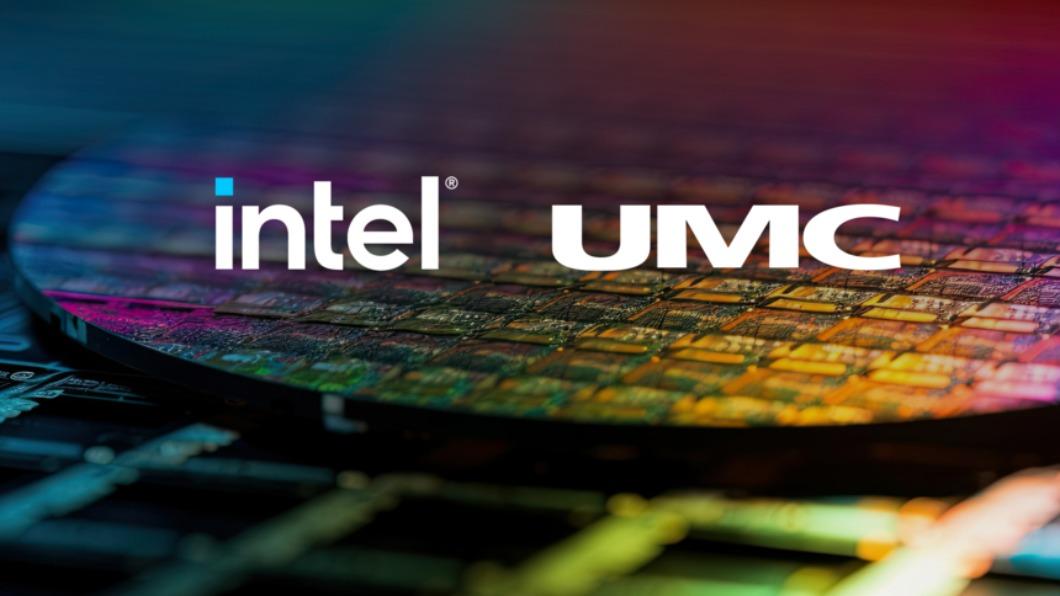
TAIPEI (TVBS News) — In a move that caught industry analysts by surprise, Intel and United Microelectronics Corporation (UMC), the second-largest foundry in Taiwan, announced plans on Thursday (Jan. 25) to join forces to develop a new 12-nanometer semiconductor manufacturing process platform for high-growth mobile, communication infrastructure, and networking markets.
The new 12nm process node will be developed and deployed by Intel Foundry Services (IFS) at Fabs 12, 22, and 32 at the Ocotillo Technology Fabrication site in Arizona. It will combine Intel's mature, high-volume manufacturing capacity and expertise in FinFET transistor design with UMC's experience in providing customers with Process Design Kit (PDK) and design assistance foundry services for customers.
Leveraging the existing equipment in the fabs will significantly reduce upfront investment requirements, minimize the carbon footprint, and optimize capacity utilization. The companies expect the new process node to become production-ready in 2027.
This collaboration is a part of Intel's broader strategy to become the world's second-largest foundry by 2030. Until now, Intel's IFS division has been able to offer only a limited range of process technologies to external customers because its fabrication processes were heavily customized for manufacturing the company's products, such as Intel Core and Intel Xeon processors.
However, to become a significant player in the foundry market, Intel has recognized the need to offer a broader range of process technologies that cater to diverse customer needs. This is where UMC's experience and substantial customer base across various sectors, including automotive and consumer electronics, become invaluable.
Collaborating with Intel to co-design a more advanced 12 nm-class process technology allows UMC to offer its customers an upgrade from its aging 14nm-class mode without independently developing a new manufacturing process and making heavy capital investments in new equipment and fabrication facilities.
The collaboration promises to be a win-win for both companies, enabling Intel to utilize its fully depreciated fabs to gain new customers and UMC to expand its capacity and market reach. It is also a sign of Intel's commitment to foster closer cooperation with Taiwan's semiconductor ecosystem to boost its capacity to meet diverse global customer needs.


