CoPoS逐步成形 台灣面板級封裝布局加速
- 作者:Richard Brown
- 發佈時間:2026.09.22 10:15
- 最後更新時間:2026.09.22 11:21
- 作者:Richard Brown
- 發佈時間:2026.09.22 10:15
- 最後更新時間:2026.09.22 11:21
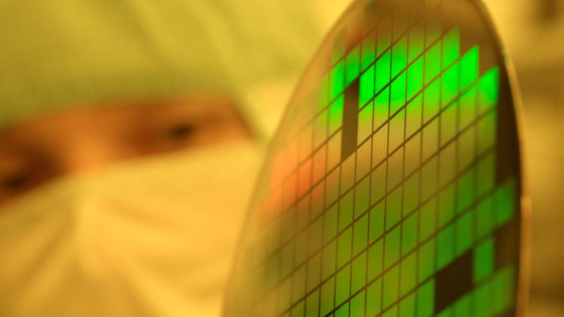
CoPoS逐步成形,台灣面板級封裝布局加速。(圖/達志影像美聯社)
台積電轉向方形面板製程,是封裝製造轉型的一環;日月光、力成與群創也正各自發展面板級封裝技術。
台積電正推動先進封裝從圓形晶圓轉向方形面板,相關工作已從規劃進入設備與材料驗證階段,讓CoPoS受到更多關注。這項轉型有望提升製造效率,但在量產之前,生產流程仍需大幅調整。台灣的專業封裝業者與顯示器製造商也正投入面板級技術,以不同的專長參與這波轉型。
CoPoS是Chip-on-Panel-on-Substrate的縮寫,是台積電在現有CoWoS(Chip-on-Wafer-on-Substrate)基礎上,朝面板級製程發展的先進封裝方案。CoWoS透過基板上的高密度互連結構,將處理器與多組高頻寬記憶體堆疊整合在一起,已成為AI硬體不可或缺的技術。然而,隨著封裝尺寸增大,在直徑300毫米的圓形晶圓上製作互連結構,面積利用效率逐漸降低。晶圓弧形邊緣的空間難以充分利用,尺寸最大的互連結構,每片晶圓可能只能容納少數幾個。
CoPoS將這部分封裝製程從圓形晶圓移至方形面板。矩形封裝可以在矩形加工表面上更有效率地排列,讓單次製程有機會同時處理更多封裝單元。更大的面板也能容納更大尺寸的互連結構,支援更多處理器、記憶體堆疊及高密度連接。實際能節省多少成本,仍取決於封裝尺寸、製造良率與加工成本。
據報導,台積電初期聚焦於310×310毫米的規格。業界消息預期,2027年進入試產,2028年下半年開始量產。這些仍是媒體引述的業界估計,並非已獲保證的生產時程。
相較於更大尺寸的面板,這個規格可作為務實的第一步。部分既有製程技術或許能經調整後沿用,但方形面板所需的搬運方式與加工配置,仍與圓形晶圓不同。尺寸接近,並不代表可以直接替換。
要讓CoPoS進入量產,從曝光、鍍銅到接合、模封與檢測,各階段設備都必須調整並完成驗證。載具、卡匣、托盤與自動化搬運系統,也都要適應方形面板。維持這些更大、更薄結構的平整度尤其困難,因為翹曲可能影響對位與加工精度。製造商必須確保整片面板上的沉積、圖案化與接合製程均勻一致,避免缺陷造成昂貴元件受損。
台積電是這波面板級封裝轉型的參與者之一。日月光、力成與群創正發展扇出型面板級封裝(FOPLP),在面板上製作延伸至個別晶片邊緣以外的電氣連接。這些製程與CoPoS在封裝結構、互連密度及目標應用上有所不同。
據報導,日月光正投資2億美元,在高雄建置大尺寸FOPLP產線,預計自2027年第一季起分階段導入。這項投資為日月光提供另一條技術路徑,以滿足客戶對更大、更複雜封裝的需求。
力成的面板級封裝技術涵蓋多種晶片與線路的製作、組裝順序。其中,「先線後晶」(chip-last)製程先製作並檢查重布線層,再放置晶片,有助於避免因互連結構有缺陷而損失良品晶片。力成將CPU、GPU及其他複雜元件列為這項技術的應用對象。其布局說明,面板級封裝不只涉及加工面積的改變,也牽涉製造順序的選擇。
群創則以不同的產業背景切入市場。公司將部分顯示面板產能轉用於FOPLP,並於2025年第二季通過客戶認證後開始出貨。群創的參與顯示,台灣在大尺寸顯示面板加工與搬運方面的經驗,可以支援半導體封裝業務的發展;不過,要滿足先進AI封裝的要求,仍需進一步提升技術能力。
在能夠大規模取代CoWoS產能之前,CoPoS將先與CoWoS形成互補。台積電必須持續擴充客戶當前需要的製程產能,同時為未來封裝開發面板級技術。日月光、力成與群創則正擴大客戶可選擇的面板級封裝方案。這些投入有望進一步提升台灣的封裝能力,但真正的商業效益,將來自讓大尺寸製程兼具可靠性與成本效益,而不只是把圓形改成方形。
CoPoS Takes Shape as Taiwan’s Panel-Packaging Industry Expands
TSMC’s move toward square-panel processing is part of a broader manufacturing shift, with ASE, Powertech, and Innolux developing their own panel-level technologies.
CoPoS is attracting greater attention as TSMC moves from planning to equipment and materials validation for its shift from round wafers to square panels in advanced packaging. The transition promises greater manufacturing efficiency, but requires substantial changes to production processes before mass production can begin. Across Taiwan, packaging specialists and display manufacturers are also investing in panel-based technologies, bringing different capabilities to this broader shift.
CoPoS, short for Chip-on-Panel-on-Substrate, is TSMC’s proposed panel-based extension of advanced packaging beyond today’s CoWoS, or Chip-on-Wafer-on-Substrate. CoWoS has become essential to AI because it brings processors and multiple stacks of high-bandwidth memory together through dense interconnect structures mounted on a substrate. As these packages grow in size, producing their interconnect structures on circular 300-millimeter wafers becomes increasingly inefficient. Space is lost around the curved edges, and only a handful of the largest structures may fit on each wafer.
CoPoS shifts this part of the packaging process from a round wafer to a square panel. Rectangular packages can be arranged more efficiently on a rectangular processing surface, potentially allowing more to be processed together. Larger panels can also accommodate larger interconnect structures supporting additional processors, memory stacks and high-density connections. The actual savings will depend on package dimensions, manufacturing yields and processing costs.
TSMC is reported to be initially concentrating on a 310-by-310-millimeter format. Industry sources expect trial production in 2027 and volume production in the second half of 2028. These remain reported industry estimates rather than a guaranteed production schedule.
That comparatively modest size could provide a practical first step before moving to substantially larger panels. Some existing process technology may be adaptable, but a square panel still requires different handling and processing arrangements from a round wafer. Similar dimensions do not make it a drop-in replacement.
Bringing CoPoS into mass production requires adapting and validating equipment for every stage, from exposure and copper plating to bonding, molding and inspection. Carriers, cassettes, trays and automated handling systems must also accommodate square panels. Keeping these larger, thinner structures flat is a particular challenge: warpage can disrupt alignment and processing accuracy. Manufacturers must maintain uniform deposition, patterning and bonding across the entire panel to prevent defects that could damage expensive components.
TSMC is one participant in a broader shift toward panel-level packaging. ASE, Powertech, and Innolux are developing fan-out panel-level packaging, or FOPLP, which forms electrical connections extending beyond the edges of individual chips across a panel. Their processes they differ from CoPoS in package structure, connection density, and target applications.
ASE is reportedly investing US$200 million in a large-format FOPLP line in Kaohsiung, with phased introduction expected from the first quarter of 2027. The investment gives the packaging group another route to serving demand for larger and more complex assemblies.
Powertech’s panel-level portfolio includes several approaches to the order in which chips and wiring are assembled. Its “chip-last” process builds and checks the redistribution wiring before adding the chips, helping to avoid losing good silicon to defective interconnect structures. The company identifies CPUs, GPUs, and other complex devices among the applications for this approach. Its work highlights how panel packaging involves choices about manufacturing sequence as well as processing area.
Innolux brings a different background to the market. It has converted display-production capacity for FOPLP and began shipments after customer qualification in the second quarter of 2025. Its participation shows how Taiwan’s experience handling large display panels can support a move into semiconductor packaging, although the requirements of advanced AI packages demand further development.
CoPoS is set to complement CoWoS before it can replace any substantial part of its production. TSMC must continue expanding the processes customers need today while developing panel technology for future packages. ASE, Powertech, and Innolux are widening the range of panel-based options available to customers. Together, these efforts could extend Taiwan’s packaging capabilities, but the commercial gains will come from making larger formats reliable and economical, not simply from changing their shape.